PCB Routing Tools: Expert Guide to Circuit Board Milling
Date:2026-02-05Number:1138PCB milling cutters represent a specialized category of machining tools designed specifically for the unique demands of printed circuit board fabrication, offering precision capabilities that bridge the gap between traditional chemical etching and modern digital manufacturing approaches. These specialized cutting instruments have transformed circuit board prototyping and low-volume production by enabling direct digital-to-physical translation of circuit designs without the chemical processing steps associated with conventional PCB manufacturing. The adoption of PCB milling technology has democratized circuit board fabrication, making rapid prototyping accessible to design engineers, research laboratories, educational institutions, and small-scale manufacturers who require quick turnaround times and design flexibility that traditional PCB production methods cannot economically provide.
The fundamental advantage of PCB milling lies in its subtractive manufacturing approach, where copper is selectively removed from clad board substrates to create circuit traces, pads, and isolation channels. This process demands cutting tools with exceptional precision, minimal runout, and specialized geometries that can produce fine features while managing the unique material characteristics of PCB substrates. Unlike conventional metalworking tools, PCB milling cutters must address the composite nature of circuit board materials—typically glass fiber reinforced epoxy substrates with thin copper cladding—while achieving the dimensional accuracy and edge quality necessary for reliable electrical connections and proper component assembly. This guide explores the technical considerations, application strategies, and tool selection factors that define successful PCB milling operations in modern electronics fabrication environments.

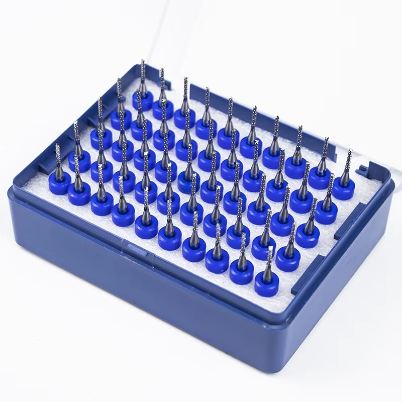
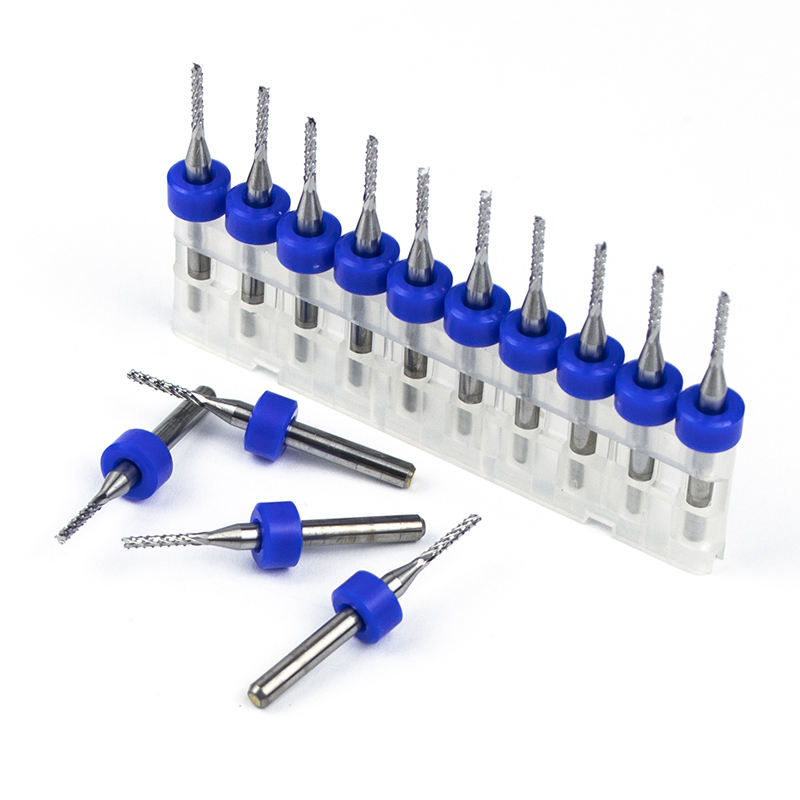
PCB milling cutter construction begins with material selection optimized for the abrasive nature of circuit board substrates while maintaining the precision necessary for fine-feature machining. Solid carbide has emerged as the predominant material choice, offering the ideal combination of hardness, wear resistance, and edge sharpness required for clean copper removal and precise substrate routing. The manufacturing process for these specialized tools involves precise grinding of micro-diameter cutting implements with tolerances significantly tighter than conventional milling tools, as even minor variations in geometry or concentricity can compromise circuit trace quality or cause trace separation failures. Tool diameters typically range from 0.1mm to 3.0mm, with the smallest sizes enabling high-density circuit routing with trace widths and spacings previously achievable only through photolithographic processes.
Geometric design represents the most critical aspect of PCB milling cutter performance, with specialized flute configurations developed specifically for circuit board materials. Single-flute designs have become standard for most PCB milling applications, providing maximum chip clearance and reduced cutting forces that minimize substrate delamination and copper tearing. The single cutting edge configuration allows for higher rotational speeds with lower vibration—a critical consideration when working with micro-diameter tools that can easily deflect or break under excessive loads. Specialized point angles and edge preparations optimize copper shearing while managing the transition between copper layer and substrate material, ensuring clean trace edges without excessive burring or material pull-up that could compromise electrical isolation or solder mask application.
Coating technologies play a significant role in extending PCB milling cutter life, particularly important given the abrasive nature of glass fiber reinforced substrates that rapidly wear conventional cutting edges. Diamond-like carbon (DLC) coatings provide exceptional hardness and lubricity, reducing friction during copper cutting while resisting the abrasive wear from glass fibers. Specialized nano-composite coatings offer enhanced performance in FR-4 and other common PCB materials, extending tool life significantly compared to uncoated alternatives. These surface treatments become increasingly valuable as tool diameters decrease, where edge wear has disproportionate effects on cutting performance and dimensional accuracy. The combination of optimized substrate materials, precision geometries, and advanced coatings creates cutting tools capable of producing professional-quality circuit boards with features approaching those achievable through commercial fabrication processes.
Isolation milling cutters represent perhaps the most common PCB milling application, where these specialized tools remove copper to create electrical isolation between circuit traces. V-cut isolation milling tools feature pointed tip geometries specifically designed to create precise isolation channels with minimal width, maximizing circuit density while ensuring reliable electrical separation. These tools typically employ 30-degree or 60-degree point angles optimized for clean copper removal without excessive substrate engagement that could cause delamination or uneven channel depths. The precision of modern isolation milling cutters enables trace separations as small as 0.2mm, supporting high-density circuit designs previously limited to commercial PCB production methods. Successful isolation milling requires careful parameter selection balancing cutting depth, feed rates, and spindle speeds to achieve clean copper removal without damaging the underlying substrate material or creating excessive burrs that could compromise electrical isolation.
Contour routing cutters address the board profiling operations that separate individual PCBs from panelized substrates or create complex board outlines. These tools feature strengthened geometries with multiple flutes (typically two or three) designed to withstand the increased engagement and cutting forces associated with full-thickness substrate cutting. Specialized chip breaker designs manage the abrasive composite dust generated during substrate routing, preventing chip packing that could lead to tool breakage or edge quality issues. Down-cut router designs provide superior surface quality on the top board surface by forcing cuttings downward rather than lifting substrate layers—a critical consideration when working with multilayer boards or materials prone to delamination. For through-hole component applications, specialized drill-mill tools combine drilling and routing capabilities, creating precise holes with clean edges that facilitate proper component insertion and soldering.
Specialized PCB milling cutters address unique fabrication requirements beyond basic isolation and profiling operations. Tapered cutters facilitate angled sidewalls for press-fit connector applications or specialized edge connections. Ball nose cutters create curved features or smooth edge transitions for specialized mechanical requirements. Engraving tools produce identification markings, component legends, or calibration patterns directly on board surfaces. Deburring tools clean edge transitions between copper and substrate materials, preparing boards for conformal coating or specialized finishing processes. Each specialized tool category serves specific niches within the broader PCB fabrication workflow, with selection depending on board design requirements, material characteristics, and production objectives that extend beyond basic circuit creation to encompass complete board preparation for assembly and deployment.

FR-4 substrate machining represents the most common PCB milling application, with this glass fiber reinforced epoxy material presenting specific challenges that influence tool selection and machining parameters. The abrasive nature of glass fibers rapidly wears cutting edges, necessitating carbide substrates and wear-resistant coatings for extended tool life. The composite structure of FR-4—with alternating layers of glass reinforcement and epoxy resin—requires cutting strategies that manage the differential wear characteristics between materials while preventing delamination between layers. Proper parameter selection balances cutting speed against fiber pull-out, with higher speeds generally producing cleaner edges but requiring careful management to prevent resin melting or thermal damage to the substrate. For multilayer board applications, specialized tools and techniques address the additional challenges of buried via formation and layer alignment while maintaining registration accuracy through the milling process.
Copper foil machining requires different approaches than substrate materials, focusing on clean shearing action rather than abrasive particle management. The ductile nature of copper presents challenges with burr formation and material pull-up, particularly problematic for fine-pitch traces where burrs can create short circuits or compromise solder mask application. Specialized cutting geometries with sharp, polished edges produce clean copper separation with minimal deformation of adjacent material. For heavy copper boards or copper substrates, modified parameters and strengthened tool geometries manage the increased material volume while maintaining edge quality. The transition between copper and substrate materials represents a critical moment in PCB milling operations, requiring tools that can effectively cut both material types without compromising performance in either—a challenge addressed through specialized edge preparations and controlled parameter adjustments during the machining process.
Alternative substrate materials including polyimide, PTFE-based RF materials, ceramic-filled composites, and metal-core boards present additional machining considerations that influence tool selection and application strategies. Polyimide films used in flexible circuits require extremely sharp cutting edges and minimal engagement to prevent material tearing or deformation. PTFE-based materials demand specialized tool geometries that manage the material's tendency to deform rather than cut cleanly. Ceramic substrates necessitate diamond-coated tools to withstand extreme abrasiveness. Aluminum and copper core boards combine metal machining requirements with dielectric layer considerations, often requiring multiple tool types and machining sequences. Each material family benefits from customized approaches developed through application experience and ongoing refinement of tool designs and machining parameters.
Cutting parameter selection represents the critical link between capable PCB milling cutters and successful circuit board fabrication, with even minor adjustments producing significant differences in edge quality, tool life, and feature accuracy. Spindle speed optimization balances several competing considerations—higher speeds generally produce cleaner cuts with reduced cutting forces but increase heat generation that can affect substrate integrity and tool life. Typical spindle speeds for PCB milling range from 20,000 to 100,000 RPM depending on tool diameter, material characteristics, and machine capabilities, with smaller diameter tools requiring proportionally higher rotational speeds to maintain effective cutting velocities. Modern PCB milling machines often incorporate high-speed spindles specifically designed for micro-tool applications, providing the rotational stability and power consistency necessary for reliable fine-feature machining.
Feed rate optimization interacts with spindle speed to determine chip load per cutting edge—a critical parameter influencing cutting forces, edge quality, and tool deflection. Conservative feed rates reduce cutting forces and tool deflection but increase machining time and may allow excessive heat generation through rubbing rather than cutting action. Aggressive feed rates improve productivity but risk tool breakage, excessive deflection, or poor edge quality. The optimal balance depends on tool diameter, tool material, substrate characteristics, and specific operation requirements, with isolation milling typically employing more conservative parameters than board profiling operations. Modern CNC controls allow dynamic feed rate adjustments during machining operations, optimizing rates for straight sections while reducing speeds for corners or direction changes where cutting conditions change abruptly.
Depth of cut strategy varies significantly between different PCB milling operations, with isolation milling typically employing shallow depths that engage only the copper layer and minimal substrate material, while board profiling operations cut through full substrate thickness. Multiple pass strategies often prove advantageous for both tool life and edge quality, particularly when working with thicker substrates or difficult materials where single-pass full-depth cutting generates excessive forces and heat. Step-down increments typically range from 0.1mm to 0.5mm depending on tool diameter and material characteristics, with smaller tools requiring more conservative approaches to prevent deflection or breakage. For isolation milling operations, depth control becomes particularly critical, as insufficient depth fails to establish proper electrical isolation while excessive depth wastes tool life and risks substrate damage that could compromise board mechanical integrity.
Process monitoring and quality control practices ensure consistent PCB milling results across production runs, particularly important for applications requiring precise impedance control or high-frequency performance. Visual inspection of milled traces under magnification reveals common issues including copper tearing, excessive burring, incomplete isolation, or substrate delamination that could compromise board functionality. Electrical continuity testing verifies isolation integrity while resistance measurements confirm proper trace dimensions and copper retention. For high-frequency or impedance-controlled applications, time-domain reflectometry or specialized testing verifies that milling processes have maintained required dimensional tolerances and edge quality. These quality assurance practices, combined with proper tool maintenance and parameter documentation, ensure that PCB milling delivers consistent results suitable for professional electronics applications ranging from prototyping through low-volume production.
Cost analysis for PCB milling operations extends beyond simple tool price comparisons to encompass total fabrication economics including material utilization, processing time, and success rates. While individual PCB milling cutters represent relatively modest investments compared to conventional metalworking tools, their specialized nature and rapid wear in abrasive PCB materials necessitate consideration of tool life and replacement frequency in overall cost calculations. The economic advantages of PCB milling emerge most clearly in prototyping and low-volume applications where conventional PCB fabrication minimum orders and lead times prove disproportionate to requirements. For these applications, the ability to produce circuit boards on-demand without chemical processing or external vendor coordination provides value that often justifies premium tooling investments and specialized equipment costs.
Implementation planning for PCB milling operations requires consideration of both technical capabilities and workflow integration. Machine selection balances precision requirements against production volume needs, with desktop PCB milling machines suitable for educational environments and light prototyping while industrial systems support higher throughput and more demanding materials. Tool management systems track cutter usage and condition, implementing preventive replacement before tool wear compromises board quality. Material handling considerations address the flatness requirements critical for successful fine-feature milling, with proper workpiece fixturing and substrate preparation often proving as important as tool selection for achieving consistent results. Software workflow integration ensures seamless transition from circuit design through toolpath generation to physical board production, with modern PCB milling systems offering increasingly sophisticated integration with common electronic design automation platforms.
The ongoing evolution of PCB milling technology continues to expand application possibilities while improving accessibility for diverse user communities. Advancements in micro-tool manufacturing enable finer features supporting higher circuit densities. Improved coating technologies extend tool life in abrasive materials. Enhanced machine designs provide greater precision and reliability. These developments, combined with growing electronics innovation across industries, ensure that PCB milling remains a vital fabrication methodology bridging the gap between circuit design conception and physical implementation. For organizations requiring rapid iteration, design confidentiality, or specialized substrates not easily accommodated by conventional PCB production, milling technology offers a compelling alternative that continues to evolve in capability and accessibility.

person: Mr. Gong
Tel: +86 0769-82380083
Mobile phone:+86 15362883951
Email: info@jimmytool.com
Website: www.jimmytool.com